
RAMCHECK LX DDR3/2
RAMCHECK LX DDR3
RAMCHECK LX DDR2
RAMCHECK LX DDR1
RAMCHECK LX Base Tester
Tech Support
Introduction
Manuals
Software Downloads
FAQ
Calibration & Upgrades
SIMCHECK II Upgrade to RAMCHECK
Application Notes
Development Logs
Service & RMA Policy
News Releases
Links
Site Map
Home
Contact us at
(281) 879-6226
sales@innoventions.com

Interpreting the RAMCHECK LX Test Log for DDR1 Devices
INN-8668-APN23
--Created 2-16-06, Updated 6-20-11
The RAMCHECK LX test log can be seen in four different ways.
- The test log will be automatically displayed after the Basic test ends unless you press the "ESC" key to terminate the test.
- You can press "F5" anytime during the Basic Test to view the test log.
- The test log can be viewed at any time after you start the Basic test by pressing the "ESC" key after the Basic test is completed. Once in standby mode press "F4" then "F1" for "View Test Log", use "F4" to go forward through the screens and "F3" to go back. Once finished press the "ESC" key to go back to standby mode.
- By installing the RAMCHECK LX PC Communications program that was included with your RAMCHECK LX on your PC and connecting your RAMCHECK LX to your computer via the USB cable (included with the package), you can view, save or print out the complete test log for future reference.
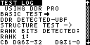 |
USING DDR PRO Detected that the DDR Pro adapter is mounted on the RAMCHECK LX. BASIC TEST The test phase used by the RAMCHECK LX. DDR DUT DETECTED - UBF Describes the type of DUT (Device Under Test) that you are testing, in this case DDR. "Type" is UNBUFFERED display as "UBF". STRUCTURE TEST Starts a brief test to determine the structure of the DDR module. All information that follows is the structure of the DDR device as detected by the RAMCHECK LX. RANK BITS DETECTED: RANK 1: CB DQ63 - 32 DQ31 - 0 |
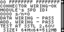 |
00 FFFFFFFF FFFFFFFF
Gives you a brief description of the structure of the DDR device by mapping the DQ and CB (Parity) bits by the module's individual ranks. This feature is very useful in troubleshooting DDR Modules with severe or multiple errors. CONNECTOR WIRING - OK At the start of the Basic Test the RAMCHECK LX performs a wiring test to verify that the control lines are properly wired and functional. In this instance it reported no errors. MODULE' s SPD ID: 0000 s/n=0 Displays the Module's Manufacturing Date in "Year/ #of weeks" and the serial number of the module that was read from the module's SPD. DATA WIRING - PASS ADD. WIRING - PASS At the start of the Basic Test the RAMCHECK LX performs a wiring test to verify that the Data and Address lines are properly wired and functional. In this case it reported no errors. TEST AT SSTL 2.60V The DDR module is being tested at 2.6 volts. SIZE: 64Mx64=512M Shows the size of the DDR module in both JEDEC notation and overall size |
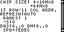 |
CHIP SIZE: 4x16Mx8 =64Mx8 Shows the size of the individual DDR chips of the DDR module in both JEDEC notation and overall size. 13 ROW/11 COL ADDR. Shows the number of rows and columns detected by the RAMCHECK LX. REFRESH:AUTO Shows that the refresh rate is in Auto mode which will use the RAMCHECK LX default value. RANKS: 1 -S:0 Shows a brief description of the structure of the DDR module similar to the "RANKS BITS DETECTED" shown above, but by displaying the number of ranks and individual control lines that were detected by the RAMCHECK LX. DQS:8..0 DM: 8..0 Detects the use of either 8/9 pairs of DQS lines and 8/9 DM lines or only 18 pairs of DQS lines. SPD=JEDEC Conforms to JEDEC standards. |
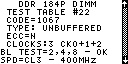 |
DDR 184P DIMM Shows the form factor of the DDR module, in this case a 184-pin DIMM. TEST TABLE #22 CODE=1067 The "TEST TABLE" and "CODE" indications are used as part of our factory development to identify certain characteristics of the DDR device. These identifications can also be used as a form of comparison to other DDR devices. TYPE: UNBUFFERED The RAMCHECK LX detected the DDR module as conforming to the JEDEC standard for UNBUFFERED configurations. Other types may include Registered, etc. ECC=N The RAMCHECK LX detected that this DDR module does not have (ECC) Error Correction Code wiring. If "ECC=Y" was displayed then ECC was detected. CLOCKS:3 CK0+1+2 The RAMCHECK LX detected the use of three clock inputs and displayed which clock inputs it detected. BL TEST=2, 4, 8 - OK The RAMCHECK LX tested the operation of the 3 burst lengths available in DDR devices, 2, 4 and 8. In this instance it indicates that BL (Burst Length) tested ok on all three. SPD=CL3 - 400MHz |
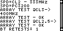 |
SPD=CL2 - 333MHz
SPD=PC3200 Any time you see "SPD=" in the test log, it always refers to the information read directly from the SPD chip on the DDR device which is programmed by the module's manufacturer. In this case the SPD claims that this module is a PC-3200 (400 MHz @ CL3). You can also view the "SPEED TEST RESULT" described below to see if the SPD information compares with the RAMCHECK test results. ARRAY TEST @CL3 400Mz Ends the "STRUCTURE TEST" and starts the "ARRAY TEST @ CL3" where the entire memory array is written and verified twice at CL=3 @ 400MHz to catch most cell stuck problems. ARRAY TEST - OK No errors were detected at CL3 @ 400MHz ARRAY TEST @CL2.5 The entire memory array is written and verified twice at CL=2.5 to catch most cell stuck problems. ARRAY TEST - OK No errors were detected at CL2.5 BT RETESTS: 1 The "BT RETEST" counter is design to catch transient or non-fatal errors that may occur randomly in memory. In this case no transient errors were found. There is also a separate counter in the "Extensive Test" called "ET RETEST". This is a comparable tool that can be used by advanced users to compare between two or more modules. Please see Application Note 33 for further details. |
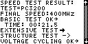 |
SPEED TEST RESULT: TEST=PC3200 The RAMCHECK LX determined that this DDR module is within PC-3200 specifications. FINAL SPEED:400MHz Final speed detected at the end of the Basic Test. BASIC TEST OK Shows that the DDR device passed the Basic Test. TIME: 00:21.5 Displays the time it took to complete the Basic Test. In this case 6.7 seconds. EXTENSIVE TEST The current test phase used by the RAMCHECK LX. STRUCTURE TEST Starts a brief test to determine the structure of the DDR module. VOLTAGE CYCLING OK |
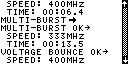 |
SPEED: 400MHz TIME: 00:06.4 Shows that the DDR module passed Voltage Cycling at 400 MHz and completed this test in 6.4 seconds from the start of the Extensive Test. Voltage Cycling is a program that cycles the test voltage while running various DDR memory tests. MULTI-BURST MULTI-BURST OK SPEED: 333 MHz TIME: 00.13.5 Multi-Burst is a proprietary technique incorporated into our DDR2 and DDR1 test engines. It enables a repeated stream of multiple data write and data read/compare memory accesses. It achieves an extremely high throughput of patterns test. (Please see Application Note 33 for further details.) VOLTAGE BOUNCE OK SPEED: 400MHz |
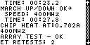 |
TIME: 00:23.2 Shows that the DDR module passed the Voltage Bounce at 400 MHz and completed the test in 9.6 seconds from the start of the Extensive Test. During Voltage Bounce, data is written to the module at a certain voltage and then read at a different voltage. MARCH UP/DOWN OK SPEED: 400MHz TIME: 00:27.8 Shows that the DDR Module passed the March Up/Down at 400 MHz and completed the test in 12.9 seconds from the start of the Extensive Test. During March Up/Down, the program attempts to catch cell interference errors. CHIP HEAT AT: 0.782A During Chip-Heat Mode, we are using our proprietary technology to heat up the module, in preparation for the final phase of the Extensive Test. 400MHz ARRAY TEST - OK No errors were detected. ET RETESTS: 2 The "ET RETEST" counter is design to catch transient or non-fatal errors that may occur randomly in memory. In this case no transient errors were found.. This is a comparable tool that can be used by advanced users to compare between two or more modules. (Please refer to Application Note 33 for further details.) . |
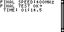 |
FINAL SPEED: 400MHz FINAL TEST OK TIME: 01:14.5 Shows that the DDR1 module passed the Final Test at 400MHz and completed the test in 1 minute and 14.5 seconds from the start of the Extensive Test. The Final Test during Extensive Test is very similar to the Basic Test. It incorporates the same two array tests but at this stage, the module has been heated up during the Extensive Test. |
CONTACTING OUR TECHNICAL SUPPORT DEPARTMENT
For more information, please call us at (281) 879-6226 M-F 9:00-5:00 US Central Time, or send your e-mail to support@innoventions.com, or fax your message to (281) 879-6415. Please remember to include your phone and e-mail.