
Thank you for visiting the RAMCHECK web
site, the original portable memory tester.
RAMCHECK DDR2 Manual Addendum
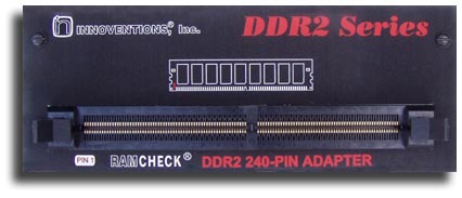
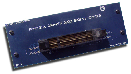
RAMCHECK LX and RAMCHECK extend their comprehensive support for testing modern DDR2 modules using the RAMCHECK DDR2 240-Pin Adapter (p/n INN-8668-15) and the RAMCHECK 200-pin DDR2 S.O. DIMM Adapter (p/n INN-8668-14). This manual addendum describes the operation of these adapters.
The only difference between the two DDR2 adapters is the test socket and target modules. Since the use of both adapters and their test flow is identical, this manual addendum use examples and screen shot taken from the DDR2 240-pin DIMM Adapter. Unless explicitly stated, all of the description and examples are also relevant to the 200-pin DDR2 SO-DIMM adapter.
NOTE: An earlier version of the DDR2 Adapter (p/n INN-8668-12) can be factory upgraded to the p/n INN-8668-15 level. Click here for the manual addendum for this older adapter.
NOTE: You must have RAMCHECK firmware version 2.67 or RAMCHECK LX firmware version 3.40 (or higher) to support the adapter. You can download the current firmware version here.
The DDR2 adapter connects to RAMCHECK via the two top 90-pin and 50-pin expansion slots. Turn RAMCHECK OFF and carefully mount the DDR2 adapter onto the RAMCHECK expansion slots, while pressing it gradually on both sides.
| CAUTION: Plug this adapter into the expansion slots only when RAMCHECK is OFF! Failure to turn RAMCHECK OFF when connecting or disconnecting the DDR2 adapter may result in damage to the internal chips of both the RAMCHECK and the adapter! |
While the DDR2 adapter is installed on RAMCHECK, you can test only the 240-pin DDR2 modules. To test the 168-pin DIMM modules (available on the older RAMCHECK tester), the DDR2 adapter must be removed. First turn the RAMCHECK OFF and carefully remove the DDR2 adapter by gradually pulling it up on both sides, taking care not to flex the adapter's boards.
| CAUTION: Please let the adapter COOL DOWN for at least 1 minute before attempting to remove it from RAMCHECK. Removal of the adapter while it is still hot may impair some of the soldered connections of its delicate internal parts! |
RAMCHECK LX automatically recognizes the presence of the DDR2 Adapter with the following initial turn-on screen:

Similarly, the older RAMCHECK automatically recognizes the presence of the DDR2 Adapter with the following initial turn-on screen:

NOTE: Throughout this on-line-manual, we use screens captured from both the newer RAMCHECK LX and from the older RAMCHECK units. The RAMCHECK LX screens are readily recognized as they are always twice the height of the RAMCHECK screens.
The DDR2 adapter supports the 240-pin DDR DIMM modules. Older 184-pin DDR1 modules are supported by our DDR PRO adapter.
INSERTION: The DDR2 adapter uses a vertically mounted high quality test socket with two ejectors that need to be opened prior to insertion. Carefully insert the DDR2 DIMM into the socket, pushing it evenly along its top. Pin 1 of the module should point to the left side (as marked on the adapter), so that the key area of the module's connector is correctly aligned with the key area in the test socket. When the DIMM is properly inserted, the ejectors will snap onto the half circle notches on each side of the module.
REMOVAL: The DIMM is easily released from the socket by pulling both ejectors sideways.
NOTE: DIMM insertion and removal should be done only when RAMCHECK is in STANDBY Mode. The RED "Module Power" LED should be OFF in STANDBY mode.
The 200-pin DDR2 SO-DIMM adapter supports the extremely delicate modules used in lap top computers. While insertion and removal proceed along the same guidelines of the previous paragraph, special care is required to avoid damage to the delicate socket. Please look at the socket very carefully to identify the narrow module entry slot before your first use. Take your time to verify the minimal force that is required to insert the module.
Turn RAMCHECK ON once the DDR2 Adapter is installed. There is no need for special setup with RAMCHECK since it automatically recognizes the DDR2 adapter. When RAMCHECK enters the STANDBY mode, the display will prompt you to test DDR2 modules. Insert the DIMM.

The DDR2 test procedure is initiated by pressing the F1 key and is designed to follow the regular RAMCHECK test flows. Unless you press the ESC key, EXTENSIVE TEST follows BASIC TEST, and AUTO-LOOP follows EXTENSIVE TEST.
The DDR2 adapter allows you to set up various test parameters like the voltage, the test frequency, and the choice of a CAS Latency. The following screens preview the BASIC TEST, showing a user-selected CAS Latency of 4 or 5. Notice that the RAMCHECK LX provides more information, regarding the test pattern and the manufacturer's speed rating.

At the start of BASIC TEST, RAMCHECK provides power and proper initialization sequence (involving control and clock lines) to the DDR2 module. A large variety of quick wiring tests are conducted, the module structure and frequency is determined, and the memory array tests begin. Since the wiring and structure tests are extremely fast, their results are logged in the Test Log and reported after the end of BASIC TEST, unless an error is encountered.
Before discussing the wiring and structure test results, let us review the main phase of the BASIC TEST, the memory array test RAMCHECK uses CL=3 for the for modules below 533MHz, and CL=4 or more for modules running at 533MHz or higher. You can use setup in the Change-on-the-Fly feature to control the CL setting. These two array tests take the bulk of the time of the BASIC TEST.
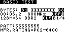
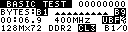
In its default setup, RAMCHECK selects CL=3 for modules that run below 533MHz and CL=4 for modules running at 533MHz and below 800MHz. At 800MHz, CL defaults to 5. You can override the CL setup. The following RAMCHECK LX screens show the information provided during the first main phase of the BASIC TEST with a typical PC2-6400 module which defaults to CL=5:
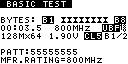
The following RAMCHECK screens show the information provided during the first main phase of the BASIC TEST with a typical PC3200 module which defaults to CL=3:
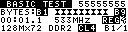
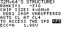
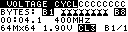
In the left example, a 32Mx72 Unbuffered (marked UBF) module is tested at CL=4 at 533MHz. The entire memory array is written and verified twice to catch most "memory cell stuck" problems. The marker to the right of the UBF message indicates that the test is set at STTL 1.8V. However, the actual voltage is automatically adjusted to 1.90V for modules running at 533MHz or higher. You can use setup or change-on-the-fly to set up your own fixed voltage selection. The two screens alternate during the test so that you can see the test voltage.
The "B1/0" marker at the bottom right corner is the "section under test" indicator, which has been modified for DDR2 devices. With DDR2 devices, each chip has four internal banks, which are selected by the BA1 and BA0 bank address lines. The module itself may have one or two main banks which are selected by S0 and S1 control lines. In this example, "B1/0" indicates that the section under test is the module's first main bank (also known as rank) and the internal chips bank 0. If the marker was "B1/1", it would indicate main bank 1 and internal chips bank 1. A "B2/3" marker indicates the second main bank (rank #2) and internal chips bank 3. Similarly, "B1/2" would indicate main bank 1 and internal chips bank 2, and so on. Modules with only one main bank will scan "B1/0"->"B1/1"-> ... ->"B1/3", before switching to the next test pattern. Modules with two main banks will scan "B1/0"-> ... ->"B1/3"->"B2/0"->...->"B2/3" for each test pattern.
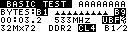
Some modules cannot run at CL=3, or are setup by the user to test at CL=4. The following screen shows the information provided during an array test at CL=4:
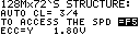
In this example, a 128Mx72 Unbuffered (marked UBF) module is tested at CL=4 at 533MHz.
Please note that a 667MHz or 533MHz modules may legitimately drop in speed during the more stringent CL2 (or CL3) CAS LATENCY array test.
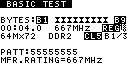
In this example (using a different module for the screen capture), a 128Mx72 Unbuffered module is tested at 400MHz and at CL=3. If testing Registered modules, the screen will look like this:
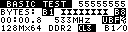
Registered modules are marked by the "REG" reversed message. In the above screen, a 128Mx72 Registered module is set up at 533Mhz. Please note that the test voltage defaults to 1.90V at such frequency. The following screen shows a registered module tested on the RAMCHECK LX:
This registered module runs at 667MHz at CL5.
At the start of the Basic Test, RAMCHECK performs a large number of wiring tests to verify that data lines, address lines and control lines are properly wired and function.
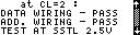
If no wiring problems are detected, the above screen is written into the Test Log. In the event of errors, RAMCHECK stops the test and provides error indication as well as detailed information regarding the pin connection associated with the detected error. Error report styles are similar to other RAMCHECK error reports for SDRAM and EDO/FPM devices. The following screens provide some examples:
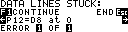
The above screen shows data line D8 (connector pin-12) stuck at logic '0'.
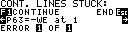
The above screen shows control line -WE (connector pin-63) stuck at logic '1'.
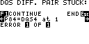
This address error example indicates an error in row address line A6 (connector pin 125) which affects some portion of the individual chips of the module. Since all address lines multiplex both rows and columns, an address error may affect ROW, COL (column) or ROW+COL. The bottom line further shows which data bits in the current bank are affected by the detected error. This allows an advanced user (e.g. a memory technician who can repair the module) to identify individual defective chips on the module. All DQ lines are divided into 4-bit groups called NIBBLES, and the hex numbers indicate which nibbles are affected by the address errors. In the above example, the nibbles code ...0303 is translated to ... 01100000011, indicating problems in nibbles 0,1,8 and 9.
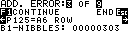
The above RAMCHECK LX screen illustrates a stuck DQS4 line at logic level '1'. It identifies the offending DQS4 line as pin 84 on the 240-pin module's connector.
RAMCHECK provides a rich set of parameters that can be changed during the BASIC TEST. We distinguish the Change-On-The-Fly setup which affects ONLY the current test from the "permanent" setup which controls the test parameters, unless changed by the user. For example, if you set up the frequency to 400MHz, then all tests will be fixed at 400MHz. If you run BASIC TEST and use the Change-On-The-Fly to set the frequency to 400MHz, then the current test will run at 400Mhz but subsequent tests will run at the regular default frequencies (or "permanent" setup frequencies). To reach the Setup menu, you press F2 during Standby mode. To activate the Change-On-The-Fly, you must first start BASIC TEST and then press F2. The following main menu will appear:
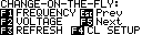
Any change done via the Change-On-The-Fly menu is relevant during the current test. Permanent setup changes can be done via the regular Setup menu, which is activated by pressing F2 during STANDBY.
Please note that the Refresh override feature is not supported on DDR2 adapters and is included in this menu in conformance with the legacy test flow of the RAMCHECK system for SDRAM and EDO/FPM tests.
The DDR2 Adapter allows you to set up the CAS LATENCY:

In the above RAMCHECK LX example, the CAS LATENCY was fixed to CL=5 throughout the tests.
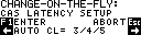
In the above RAMCHECK example, the CAS LATENCY was fixed to automatic selection of CL. DDR2 supports CL of 2,3,4,5 and 6.

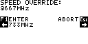
The DDR2 VDD Voltage setup allows the user to change on-the-fly the test voltage in the range 1.5V-2.2V. When set to AUTO, RAMCHECK automatically tests the module at 1.8V/1.9V.
You can use the change-on-the-fly to modify the test frequency.
RAMCHECK LX provides detailed test results upon the completion of the Basic Test phase:

The following screens lists the test results. Please note that you can hold and release the current screens by pressing F3 and F4. The test results are also captured into the RAMCHECK Test Log, as described in the following section.
The following RAMCHECK screen shows the first summary screen following a successful Basic Test with another module:

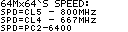
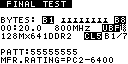
In this example, a DDR2 1GB module, organized as 128Mx72, was tested at 400MHz. The module was of the Unbuffered type (UBF message), tested at 1.8V (like all DDR2 devices), and it uses 3 differential clock pairs.
RAMCHECK Basic Test provides several screens for test results. The third structure screen shown here includes some of the new features of the DDR2, including the CAS LATENCY and the voltage setup.
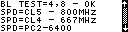
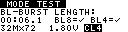
During the Basic Test, RAMCHECK tests the operation of the two Burst Length available in DDR2 devices - 4 and 8. Unlike older SDRAM, new DDR2 devices do not support burst length of 2 and Full Page Burst. The following screen shows a summary screen indicating that BL (Burst Length) was tested OK:

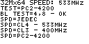
During the Basic Test, RAMCHECK interrogates the SPD of the module to read the maximum declared frequency as based on the various CL settings:
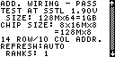
The above example shows the reading from a PC2-6400 DDR2 module. Such a module can reach 667MHz at CL4 and 800MHz at CL5. The adapter tests this module at a maximum of 866MHz.
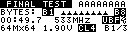
Here is another example where the CAS LATENCY was set automatically to 3 or 4 depending on the test frequency. The example also includes an ECC DDR2 module and the test voltage was maintained at 1.8V.
The RAMCHECK Test Log allows you to review all of the DDR2 test results in one continuous scrolling display. You can view the test even after the test ends (but before you start a new test) by pressing F3 from Standby and selecting Test Log with F1. The Test Log is one of RAMCHECK's most powerful features. When used with the PC Communications program, the test log can be printed and saved into convenient log files.
The following screens shows you some of the new features of the DDR2 adapter as seen in the RAMCHECK LX Test Log.
The Test Log lists the initial wiring tests and the size measurement results.
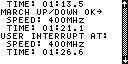
In the above screen, the test completed MARCH UP/DOWN at 400MHz before being interrupted by the user pressing the 'ESC' button.
Several new RTT test results are listed in the above screen.
The following screens shows you some of the older RAMCHECK test logs.

Numerous wiring tests are executed at the start of the Basic Test. This screen illustrates some of these results in the test log.
This screen shows the detailed structure of the chip comprising the DDR2 module. It also indicates the actual test voltage.
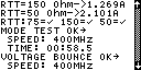
This screen shows the SPD marking of the module speed at CL5 and CL4. Please note that the module's maximum speed may legitimately drop in speed during the more stringent CL array tests..
This screen demonstrates that the results from the DDR2 Extensive Test. The Voltage Bounce test has been completed successfully.
DDR2 memory devices use data read/write strobe signals (DQS) as well as Data Mask (DM) signals for masking write activity on the selected chip. The DQS for DDR2 come as a differential pairs, and they control the transfer of data from and to the memory device. When the DM signal is set high, the attached DDR2 device will not accept data which is written to it, that is, the written data is masked out from changing the memory device contents. The 240-pin connector includes either 9 pairs of DQS lines and 9 DM lines or only 18 pairs of DQS lines. The DDR2 adapter set the DQS pairs in accordance with the differential SSTL1.8 standard. Some tests can set the DDR2 devices for single DQS lines.
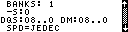
Most DDR2 modules are made of x8 type DDR chips and they are wired to use 9/8 DQS lines (9 for x72 ECC DIMMs, only 8 for x64 DIMMs). They also use 9/8 DM lines. Such modules are identified in RAMCHECK's Test Log with the line "DQS:08..0 DM:08..0" as depicted in the following screen:
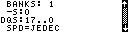
Some Registered modules which are made of x4 type DDR2 chips are wired to 18/16 DQS lines (18 for x72 ECC DIMMs, only 16 for x64 DIMMs). The DM control line of the DDR2 chips of such modules are disabled by a fixed connection to ground. Such modules are identified in RAMCHECK's Test Log with the line "DQS:17..0" as shown in the following screen:
You can permanently change test parameters using the RAMCHECK Setup Menu. You reach Setup by pressing F2 from Standby mode. Press F1 to select Parameter Setup. Setup parameter menus are similar to the Change-On-The-Fly menus discussed above.
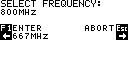
The following RAMCHECK LX screen shows the DDR2 Frequency Setup:
The following RAMCHECK screen shows the DDR2 Voltage Setup:
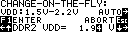
Unlike the CHANGE-ON-THE-FLY above where the new voltage setup is effective for one test, you can use the Setup Parameters to change the test voltage parameters for all tests.
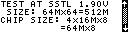
DDR2 EXTENSIVE TESTThe EXTENSIVE TEST for DDR2 is similar to our DDR1 and SDRAM tests. Currently, the following test phases are performed:
During Voltage Cycling, the program cycles the test voltage while running various DDR2 memory tests. Some frequency drifts are normal for this test, as the module is periodically run at its lower voltage margin. The test can be skipped by pressing F1, or run again by pressing F2.
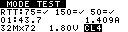
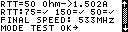
The new Mode Test explicitly checks various parameters of the DDR2 device. Currently it includes tests for the Burst Length, CAS Latency, Additive Latency and the Rtt/ODT controlled termination. (Please note that you must have firmware 2.30 or higher for this test).
Burst Length
DDR2 support Burst Lengths (BL) of 8 and 4. The Burst Length of 2 which is supported by SDRAM and DDR1 is not supported by DDR2 and future DDR generations.
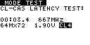
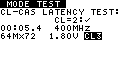
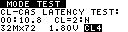
CAS Latency
Please note that CAS Latency (CL) of 2 and 6 are optional, while all DDR2 devices must support CL of 3,4, and 5. The following screen shows a module that does not support CL2.
|

|
|
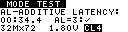
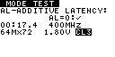
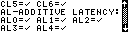
Additive Latency
DDR2 devices should support Additive Latency (AL) of 0,1,2,3,and 4. The following screen shows the test result for AL=3.
In this RAMCHECK LX screen, the AL value is tested at AL=0;
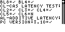
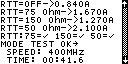
Rtt/ODT On-Die-Termination Test
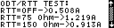
The DDR2 devices employ a novel approach of built-in controlled termination, called On-Die-Termination (ODT). The ODT feature is controlled by a pair of input lines (ODT0 and ODT1), and special setup of the termination resistance Rtt. The Rtt setup supported by DDR2 technology is OFF, 75 Ohm, 150 Ohm and 50 Ohm. Please note that some devices do not support the 50 Ohm setup (they respond with 75 Ohm when the system is configured for 50 Ohm). We use our state-of-the-art current consumption/impedence determination circuitry to test the Rtt/ODT feature. The following screen shows the summary result for a module that supports all Rtt setup.
The following RAMCHECK LX screen illustrates the Rtt/ODT test in progress, showing the current consumed at the time the test was set for ODT=1 and RTT=OFF.

Detailed Mode results in the Test Log
Since the Mode Test includes a variety of sub-tests, many of which are very fast, the program Test Log is a very useful review tool. In the following RAMCHECK LX screens we captured a complete set of the Mode test results to demonstrate the extensive detail.
|
|
|
|
The following RAMCHECK screens show a similar set of the Mode test results:

|
|
|
|
|
|
|

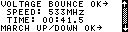
During Voltage Bounce, data is written to the module at a certain voltage (e.g. 1.95V) and then read at a different voltage (e.g. 1.75V). Some frequency drifts are normal for this test, as the module is periodically run at its lower voltage margin. The test can be skipped by pressing F1, or run again by pressing F2.


During March Up/Down, the program attempts to catch cell interference errors. The test can be skipped by pressing F1, or run again by pressing F2.

During Chip-Heat Mode, we are using our proprietary technology to heat up the module, in preparation for the final phase of the Extensive Test. This mode can be skipped by pressing F1, or run again by pressing F2.
The Final Test during Extensive Test is very similar to Basic Test. It incorporates the same two array tests. Typically, at this stage, the module has been heated up during Extensive Test and the Chip Heat Mode. This test can be repeated by pressing F2.
The AUTO-LOOP test uses changing patterns to burn-in the module and to detect cell interferences. AUTO-LOOP continues until an error is detected or the user terminates the test by pressing the ESC key.
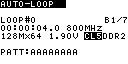

The AUTO-LOOP screen indicates the current loop number and the first data of the current complex pattern. Note that each complex pattern includes an 8x72 bit array, so that the "AAAAAAAA" hex marker is just the first 32 bits of the first 64/72 bit extended word.
The screen also shows the voltage, the CL setup and current portion of the module that is being tested ("B1/1" means chip bank 1 of rank 1). Unless you have selected a specific CAS Latency (CL) value, the program automatically changes the CL setup every few loops. Similarly, unless you have setup a fixed voltage, the test voltages change every few loops. You can skip loops using F1, cycle the voltage using F2, or cycle the CL setup using F5.


During AUTO-LOOP, the program automatically cools down the tested module every 16 loops, so that the module's operation is checked with a changing temperature gradient. Other functions like self refresh or cke controlled power down mode are exercised during the cool down period.
INNOVENTIONS, Inc., reserves the right to change products or specifications without prior notice.