Thank you for visiting the RAMCHECK web
site, the original portable memory tester.
How To Repair RAM
The RAMCHECK LX memory tester is a powerful tool for repairing defective DIMM and SODIMM modules by pinpointing the defect and identifying the defective chip. Of course, the first thing you need to do is test the suspect module to confirm that it is faulty. This takes just a few seconds with RAMCHECK LX.
RAMCHECK LX will quickly identify the module's speed, size and type, and give a pass/fail message. RAMCHECK LX error messages also generally identify the relevant pins (circuit connections to the test socket) of the module being tested which are associated with the problem. It is designed to provide you with explicit error data to enable you to identify the defective component(s) on the module.
RAMCHECK
LX DETAILED ERROR MESSAGES
|
||||||||||||||||
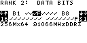
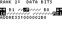
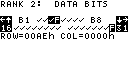
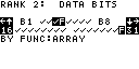
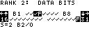
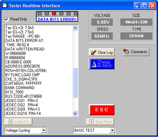
When RAMCHECK LX reports a data bit error, it tells you which DQ bit/s are bad and it also identifies the relevant pins (circuit connections to the test socket) of the module which are associated with the bad bits. You can remove the module from the socket and review the Test Log of the last memory test by pressing F4 during Standby. Easier still, use the RAMCHECK PC interface to identify faults (see below).
Every memory module has chips that are arranged from left to right (when you look at rank 1) in accordance with the bits (each bit has a DQ number) of the module. RAMCHECK LX data errors clearly identify the DQ bit/s which are bad and it tells you which chips are being used. You can easily identify the bad chip from the RAMCHECK LX data errors as follows.
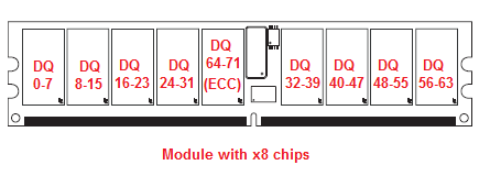
The most popular modules (regardless of size and DDR1/2/3 type) use individual chips with x8 data width. Therefore, x64 module uses 8 such chips per rank and ECC (x72) uses 9 chips. The first chip on the left always connects to DQ0-7. The second chip connects to DQ8-15, the third chip from the left connects to DQ16-23, and so forth. The ECC chip (for DQ64-71), if available, is placed in the middle of the module as the 5th chip, as shown in the following drawing.
For example, if RAMCHECK LX reports the error DQ17 bad, you know it is the third chip (DQ16-23) from the left. If you test a dual rank module (one that has chips in both sides), you need to follow the RANK number reported by RAMCHECK LX. If it is RANK 2, you need to turn the module over and follow the chips in a reversed order - DQ0-7 of RANK 2 will be the first chip on the right side when you look at the back side of the module.
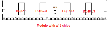
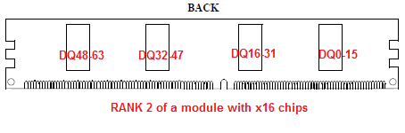
Similarly, an x64 data width module (regardless of size) that uses x16 data width individual chips, has 4 chips per rank. The first chip on the left always connects to DQ0-15. The second chip connects to DQ16-31, the third chip from the left connects to DQ32-47, and so forth, as shown in the following drawing. So if for example RAMCHECK LX reports the error DQ30 bad in RANK 1, you know it is the second chip.
If RAMCHECK reports DQ30 in RANK 2, the bad chip will be the second from the right when you look at the back side of the module, as shown here
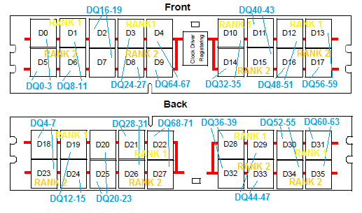
Server ECC x72 modules with x4 chips also have a regular orderly arrangement and your technician can convert the RAMCHECK LX error report to identify the chips. Such module are typically include 36 chips, for two RANKS. The following drawing illustrates how the chips are connected. The chips marked D0-D4, D10-D13, D18-D22 and D28 to D31 comprise RANK 1. The chips marked D5-D9, D14-D17, D23-D27 and D32-D35 comprise RANK 2 of the module. The vertical chips pairs (e.g D0 and D5, D1 and D6, etc.) connect in parallel, and control by module control lines S0 (for RANK 1) or S1 (for RANK 2).
Chips D0 and D5 connects to DQ0-3 in the front of the module. Chips D18 and D23, which are placed directly beneath D0 and D5 on the back of the module, connect to DQ4-7. Continuing in this order, chips D1 and D6 connect to DQ8-11 on the front side of the module. Chips D19 and D24 on the back of the module connect to DQ12-15, and so on. Finally, the last chip pair in the front side (D13 and D17) connect to DQ56-59 while the chips D31 and D35 beneath them on the back side of the module connect to DQ60-63.
Server ECC x72 modules with x4 chips and only one rank are much less popular. The arrangement of the chips is similar to the above drawing, with the omission of chips D5-D9, D14-D17, D23-D27 and D32-35. More explicit drawings of modules is available in the JEDEC web site, but the above drawing should be sufficient to determine the chips in most cases.
Now that you know where the defective chip is you'll have to replace it. Only a technician with component-level repair expertise can repair a memory module. The required soldering/ desoldering equipment is relatively complex, especially with modules and cards made with extremely thin Surface Mount Technology (i.e., devices with BGA or TSOP chips).
You will need a good deal of practice with desoldering techniques. Nevertheless, a few minor problems, which are identified by RAMCHECK, can be repaired with simple tools. A short between an adjacent pin may be caused by a small piece of metallic debris, which is stuck between two chips. You "repair" the module in this case with an Exacto knife or a watchmaker's fine screwdriver by simply removing the debris. If you use RAMCHECK in the production shop, you should be able to easily replace the module's components.
Repairing memory does involve a fair amount of work, but
as companies around the world have discovered with
RAMCHECK LX, it can be a lucrative business.
Structure analysis for RAMCHECK test results - important for memory module repair.